2.5: Electrons and “holes’’
- Page ID
- 739
\( \newcommand{\vecs}[1]{\overset { \scriptstyle \rightharpoonup} {\mathbf{#1}} } \)
\( \newcommand{\vecd}[1]{\overset{-\!-\!\rightharpoonup}{\vphantom{a}\smash {#1}}} \)
\( \newcommand{\id}{\mathrm{id}}\) \( \newcommand{\Span}{\mathrm{span}}\)
( \newcommand{\kernel}{\mathrm{null}\,}\) \( \newcommand{\range}{\mathrm{range}\,}\)
\( \newcommand{\RealPart}{\mathrm{Re}}\) \( \newcommand{\ImaginaryPart}{\mathrm{Im}}\)
\( \newcommand{\Argument}{\mathrm{Arg}}\) \( \newcommand{\norm}[1]{\| #1 \|}\)
\( \newcommand{\inner}[2]{\langle #1, #2 \rangle}\)
\( \newcommand{\Span}{\mathrm{span}}\)
\( \newcommand{\id}{\mathrm{id}}\)
\( \newcommand{\Span}{\mathrm{span}}\)
\( \newcommand{\kernel}{\mathrm{null}\,}\)
\( \newcommand{\range}{\mathrm{range}\,}\)
\( \newcommand{\RealPart}{\mathrm{Re}}\)
\( \newcommand{\ImaginaryPart}{\mathrm{Im}}\)
\( \newcommand{\Argument}{\mathrm{Arg}}\)
\( \newcommand{\norm}[1]{\| #1 \|}\)
\( \newcommand{\inner}[2]{\langle #1, #2 \rangle}\)
\( \newcommand{\Span}{\mathrm{span}}\) \( \newcommand{\AA}{\unicode[.8,0]{x212B}}\)
\( \newcommand{\vectorA}[1]{\vec{#1}} % arrow\)
\( \newcommand{\vectorAt}[1]{\vec{\text{#1}}} % arrow\)
\( \newcommand{\vectorB}[1]{\overset { \scriptstyle \rightharpoonup} {\mathbf{#1}} } \)
\( \newcommand{\vectorC}[1]{\textbf{#1}} \)
\( \newcommand{\vectorD}[1]{\overrightarrow{#1}} \)
\( \newcommand{\vectorDt}[1]{\overrightarrow{\text{#1}}} \)
\( \newcommand{\vectE}[1]{\overset{-\!-\!\rightharpoonup}{\vphantom{a}\smash{\mathbf {#1}}}} \)
\( \newcommand{\vecs}[1]{\overset { \scriptstyle \rightharpoonup} {\mathbf{#1}} } \)
\( \newcommand{\vecd}[1]{\overset{-\!-\!\rightharpoonup}{\vphantom{a}\smash {#1}}} \)
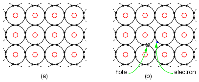
\(\newcommand{\avec}{\mathbf a}\) \(\newcommand{\bvec}{\mathbf b}\) \(\newcommand{\cvec}{\mathbf c}\) \(\newcommand{\dvec}{\mathbf d}\) \(\newcommand{\dtil}{\widetilde{\mathbf d}}\) \(\newcommand{\evec}{\mathbf e}\) \(\newcommand{\fvec}{\mathbf f}\) \(\newcommand{\nvec}{\mathbf n}\) \(\newcommand{\pvec}{\mathbf p}\) \(\newcommand{\qvec}{\mathbf q}\) \(\newcommand{\svec}{\mathbf s}\) \(\newcommand{\tvec}{\mathbf t}\) \(\newcommand{\uvec}{\mathbf u}\) \(\newcommand{\vvec}{\mathbf v}\) \(\newcommand{\wvec}{\mathbf w}\) \(\newcommand{\xvec}{\mathbf x}\) \(\newcommand{\yvec}{\mathbf y}\) \(\newcommand{\zvec}{\mathbf z}\) \(\newcommand{\rvec}{\mathbf r}\) \(\newcommand{\mvec}{\mathbf m}\) \(\newcommand{\zerovec}{\mathbf 0}\) \(\newcommand{\onevec}{\mathbf 1}\) \(\newcommand{\real}{\mathbb R}\) \(\newcommand{\twovec}[2]{\left[\begin{array}{r}#1 \\ #2 \end{array}\right]}\) \(\newcommand{\ctwovec}[2]{\left[\begin{array}{c}#1 \\ #2 \end{array}\right]}\) \(\newcommand{\threevec}[3]{\left[\begin{array}{r}#1 \\ #2 \\ #3 \end{array}\right]}\) \(\newcommand{\cthreevec}[3]{\left[\begin{array}{c}#1 \\ #2 \\ #3 \end{array}\right]}\) \(\newcommand{\fourvec}[4]{\left[\begin{array}{r}#1 \\ #2 \\ #3 \\ #4 \end{array}\right]}\) \(\newcommand{\cfourvec}[4]{\left[\begin{array}{c}#1 \\ #2 \\ #3 \\ #4 \end{array}\right]}\) \(\newcommand{\fivevec}[5]{\left[\begin{array}{r}#1 \\ #2 \\ #3 \\ #4 \\ #5 \\ \end{array}\right]}\) \(\newcommand{\cfivevec}[5]{\left[\begin{array}{c}#1 \\ #2 \\ #3 \\ #4 \\ #5 \\ \end{array}\right]}\) \(\newcommand{\mattwo}[4]{\left[\begin{array}{rr}#1 \amp #2 \\ #3 \amp #4 \\ \end{array}\right]}\) \(\newcommand{\laspan}[1]{\text{Span}\{#1\}}\) \(\newcommand{\bcal}{\cal B}\) \(\newcommand{\ccal}{\cal C}\) \(\newcommand{\scal}{\cal S}\) \(\newcommand{\wcal}{\cal W}\) \(\newcommand{\ecal}{\cal E}\) \(\newcommand{\coords}[2]{\left\{#1\right\}_{#2}}\) \(\newcommand{\gray}[1]{\color{gray}{#1}}\) \(\newcommand{\lgray}[1]{\color{lightgray}{#1}}\) \(\newcommand{\rank}{\operatorname{rank}}\) \(\newcommand{\row}{\text{Row}}\) \(\newcommand{\col}{\text{Col}}\) \(\renewcommand{\row}{\text{Row}}\) \(\newcommand{\nul}{\text{Nul}}\) \(\newcommand{\var}{\text{Var}}\) \(\newcommand{\corr}{\text{corr}}\) \(\newcommand{\len}[1]{\left|#1\right|}\) \(\newcommand{\bbar}{\overline{\bvec}}\) \(\newcommand{\bhat}{\widehat{\bvec}}\) \(\newcommand{\bperp}{\bvec^\perp}\) \(\newcommand{\xhat}{\widehat{\xvec}}\) \(\newcommand{\vhat}{\widehat{\vvec}}\) \(\newcommand{\uhat}{\widehat{\uvec}}\) \(\newcommand{\what}{\widehat{\wvec}}\) \(\newcommand{\Sighat}{\widehat{\Sigma}}\) \(\newcommand{\lt}{<}\) \(\newcommand{\gt}{>}\) \(\newcommand{\amp}{&}\) \(\definecolor{fillinmathshade}{gray}{0.9}\)Figure below (a) shows four electrons in the valence shell of a semiconductor forming covalent bonds to four other atoms. This is a flattened, easier to draw, version of Figure above. All electrons of an atom are tied up in four covalent bonds, pairs of shared electrons. Electrons are not free to move about the crystal lattice. Thus, intrinsic, pure, semiconductors are relatively good insulators as compared to metals.

(a) Intrinsic semiconductor is an insulator having a complete electron shell. (b) However, thermal energy can create few electron hole pairs resulting in weak conduction.
Thermal energy may occasionally free an electron from the crystal lattice as in Figure above (b). This electron is free for conduction about the crystal lattice. When the electron was freed, it left an empty spot with a positive charge in the crystal lattice known as a hole. This hole is not fixed to the lattice; but, is free to move about. The free electron and hole both contribute to conduction about the crystal lattice. That is, the electron is free until it falls into a hole. This is called recombination. If an external electric field is applied to the semiconductor, the electrons and holes will conduct in opposite directions. Increasing temperature will increase the number of electrons and holes, decreasing the resistance. This is opposite of metals, where resistance increases with temperature by increasing the collisions of electrons with the crystal lattice. The number of electrons and holes in an intrinsic semiconductor are equal. However, both carriers do not necessarily move with the same velocity with the application of an external field. Another way of stating this is that the mobility is not the same for electrons and holes.
Pure semiconductors, by themselves, are not particularly useful. Though, semiconductors must be refined to a high level of purity as a starting point prior the addition of specific impurities.
Semiconductor material pure to 1 part in 10 billion, may have specific impurities added at approximately 1 part per 10 million to increase the number of carriers. The addition of a desired impurity to a semiconductor is known as doping. Doping increases the conductivity of a semiconductor so that it is more comparable to a metal than an insulator.
It is possible to increase the number of negative charge carriers within the semiconductor crystal lattice by doping with an electron donor like Phosphorus. Electron donors, also known as N-type dopants include elements from group VA of the periodic table: nitrogen, phosphorus, arsenic, and antimony. Nitrogen and phosphorus are N-type dopants for diamond. Phosphorus, arsenic, and antimony are used with silicon.
The crystal lattice in Figure below (b) contains atoms having four electrons in the outer shell, forming four covalent bonds to adjacent atoms. This is the anticipated crystal lattice. The addition of a phosphorus atom with five electrons in the outer shell introduces an extra electron into the lattice as compared with the silicon atom. The pentavalent impurity forms four covalent bonds to four silicon atoms with four of the five electrons, fitting into the lattice with one electron left over. Note that this spare electron is not strongly bonded to the lattice as the electrons of normal Si atoms are. It is free to move about the crystal lattice, not being bound to the Phosphorus lattice site. Since we have doped at one part phosphorus in 10 million silicon atoms, few free electrons were created compared with the numerous silicon atoms. However, many electrons were created compared with the fewer electron-hole pairs in intrinsic silicon. Application of an external electric field produces strong conduction in the doped semiconductor in the conduction band (above the valence band). A heavier doping level produces stronger conduction. Thus, a poorly conducting intrinsic semiconductor has been converted into a good electrical conductor.

(a) Outer shell electron configuration of donor N-type Phosphorus, Silicon (for reference), and acceptor P-type Boron. (b) N-type donor impurity creates free electron (c) P-type acceptor impurity creates hole, a positive charge carrier.
It is also possible to introduce an impurity lacking an electron as compared with silicon, having three electrons in the valence shell as compared with four for silicon. In Figure above (c), this leaves an empty spot known as a hole, a positive charge carrier. The boron atom tries to bond to four silicon atoms, but only has three electrons in the valence band. In attempting to form four covalent bonds the three electrons move around trying to form four bonds. This makes the hole appear to move. Furthermore, the trivalent atom may borrow an electron from an adjacent (or more distant) silicon atom to form four covalent bonds. However, this leaves the silicon atom deficient by one electron. In other words, the hole has moved to an adjacent (or more distant) silicon atom. Holes reside in the valence band, a level below the conduction band. Doping with an electron acceptor, an atom which may accept an electron, creates a deficiency of electrons, the same as an excess of holes. Since holes are positive charge carriers, an electron acceptor dopant is also known as a P-type dopant. The P-type dopant leaves the semiconductor with an excess of holes, positive charge carriers. The P-type elements from group IIIA of the periodic table include: boron, aluminum, gallium, and indium. Boron is used as a P-type dopant for silicon and diamond semiconductors, while indium is used with germanium.
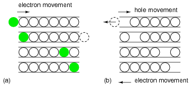
The “marble in a tube” analogy to electron conduction in Figure below relates the movement of holes with the movement of electrons. The marble represent electrons in a conductor, the tube. The movement of electrons from left to right as in a wire or N-type semiconductor is explained by an electron entering the tube at the left forcing the exit of an electron at the right. Conduction of N-type electrons occurs in the conduction band. Compare that with the movement of a hole in the valence band.

Marble in a tube analogy: (a) Electrons move right in the conduction band as electrons enter tube. (b) Hole moves right in the valence band as electrons move left.
For a hole to enter at the left of Figure above (b), an electron must be removed. When moving a hole left to right, the electron must be moved right to left. The first electron is ejected from the left end of the tube so that the hole may move to the right into the tube. The electron is moving in the opposite direction of the positive hole. As the hole moves farther to the right, electrons must move left to accommodate the hole. The hole is the absence of an electron in the valence band due to P-type doping. It has a localized positive charge. To move the hole in a given direction, the valence electrons move in the opposite direction.
Electron flow in an N-type semiconductor is similar to electrons moving in a metallic wire. The N-type dopant atoms will yield electrons available for conduction. These electrons, due to the dopant are known as majority carriers, for they are in the majority as compared to the very few thermal holes. If an electric field is applied across the N-type semiconductor bar in Figure below (a), electrons enter the negative (left) end of the bar, traverse the crystal lattice, and exit at right to the (+) battery terminal.

(a) N-type semiconductor with electrons moving left to right through the crystal lattice. (b) P-type semiconductor with holes moving left to right, which corresponds to electrons moving in the opposite direction.
Current flow in a P-type semiconductor is a little more difficult to explain. The P-type dopant, an electron acceptor, yields localized regions of positive charge known as holes. The majority carrier in a P-type semiconductor is the hole. While holes form at the trivalent dopant atom sites, they may move about the semiconductor bar. Note that the battery in Figure above (b) is reversed from (a). The positive battery terminal is connected to the left end of the P-type bar. Electron flow is out of the negative battery terminal, through the P-type bar, returning to the positive battery terminal. An electron leaving the positive (left) end of the semiconductor bar for the positive battery terminal leaves a hole in the semiconductor, that may move to the right. Holes traverse the crystal lattice from left to right. At the negative end of the bar an electron from the battery combines with a hole, neutralizing it. This makes room for another hole to move in at the positive end of the bar toward the right. Keep in mind that as holes move left to right, that it is actually electrons moving in the opposite direction that is responsible for the apparant hole movement.
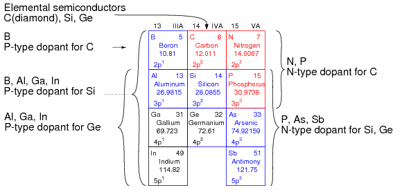
The elements used to produce semiconductors are summarized in Figure below. The oldest group IVA bulk semiconductor material germanium is only used to a limited extent today. Silicon based semiconductors account for about 90% of commercial production of all semiconductors. Diamond based semiconductors are a research and development activity with considerable potential at this time. Compound semiconductors not listed include silicon germanium (thin layers on Si wafers), silicon carbide and III-V compounds such as gallium arsenide. III-VI compound semiconductors include: AlN, GaN, InN, AlP, AlAs, AlSb, GaP, GaAs, GaSb, InP, InAs, InSb, AlxGa1-xAs and InxGa1-xAs. Columns II and VI of periodic table, not shown in the figure, also form compound semiconductors.

Group IIIA P-type dopants, group IV basic semiconductor materials, and group VA N-type dopants.
The main reason for the inclusion of the IIIA and VA groups in Figure above is to show the dopants used with the group IVA semiconductors. Group IIIA elements are acceptors, P-type dopants, which accept electrons leaving a hole in the crystal lattice, a positive carrier. Boron is the P-type dopant for diamond, and the most common dopant for silicon semiconductors. Indium is the P-type dopant for germanium.
Group VA elements are donors, N-type dopants, yielding a free electron. Nitrogen and Phosphorus are suitable N-type dopants for diamond. Phosphorus and arsenic are the most commonly used N-type dopants for silicon; though, antimony can be used.
Review
- Intrinsic semiconductor materials, pure to 1 part in 10 billion, are poor conductors.
- N-type semiconductor is doped with a pentavalent impurity to create free electrons. Such a material is conductive. The electron is the majority carrier.
- P-type semiconductor, doped with a trivalent impurity, has an abundance of free holes. These are positive charge carriers. The P-type material is conductive. The hole is the majority carrier.
- Most semiconductors are based on elements from group IVA of the periodic table, silicon being the most prevalent. Germanium is all but obsolete. Carbon (diamond) is being developed.
- Compound semiconductors such as silicon carbide (group IVA) and gallium arsenide (group III-V) are widely used.


