
3.12: Special-purpose Diodes
- Page ID
- 1773

\( \newcommand{\vecs}[1]{\overset { \scriptstyle \rightharpoonup} {\mathbf{#1}} } \)
\( \newcommand{\vecd}[1]{\overset{-\!-\!\rightharpoonup}{\vphantom{a}\smash {#1}}} \)
\( \newcommand{\id}{\mathrm{id}}\) \( \newcommand{\Span}{\mathrm{span}}\)
( \newcommand{\kernel}{\mathrm{null}\,}\) \( \newcommand{\range}{\mathrm{range}\,}\)
\( \newcommand{\RealPart}{\mathrm{Re}}\) \( \newcommand{\ImaginaryPart}{\mathrm{Im}}\)
\( \newcommand{\Argument}{\mathrm{Arg}}\) \( \newcommand{\norm}[1]{\| #1 \|}\)
\( \newcommand{\inner}[2]{\langle #1, #2 \rangle}\)
\( \newcommand{\Span}{\mathrm{span}}\)
\( \newcommand{\id}{\mathrm{id}}\)
\( \newcommand{\Span}{\mathrm{span}}\)
\( \newcommand{\kernel}{\mathrm{null}\,}\)
\( \newcommand{\range}{\mathrm{range}\,}\)
\( \newcommand{\RealPart}{\mathrm{Re}}\)
\( \newcommand{\ImaginaryPart}{\mathrm{Im}}\)
\( \newcommand{\Argument}{\mathrm{Arg}}\)
\( \newcommand{\norm}[1]{\| #1 \|}\)
\( \newcommand{\inner}[2]{\langle #1, #2 \rangle}\)
\( \newcommand{\Span}{\mathrm{span}}\) \( \newcommand{\AA}{\unicode[.8,0]{x212B}}\)
\( \newcommand{\vectorA}[1]{\vec{#1}} % arrow\)
\( \newcommand{\vectorAt}[1]{\vec{\text{#1}}} % arrow\)
\( \newcommand{\vectorB}[1]{\overset { \scriptstyle \rightharpoonup} {\mathbf{#1}} } \)
\( \newcommand{\vectorC}[1]{\textbf{#1}} \)
\( \newcommand{\vectorD}[1]{\overrightarrow{#1}} \)
\( \newcommand{\vectorDt}[1]{\overrightarrow{\text{#1}}} \)
\( \newcommand{\vectE}[1]{\overset{-\!-\!\rightharpoonup}{\vphantom{a}\smash{\mathbf {#1}}}} \)
\( \newcommand{\vecs}[1]{\overset { \scriptstyle \rightharpoonup} {\mathbf{#1}} } \)
\( \newcommand{\vecd}[1]{\overset{-\!-\!\rightharpoonup}{\vphantom{a}\smash {#1}}} \)
\(\newcommand{\avec}{\mathbf a}\) \(\newcommand{\bvec}{\mathbf b}\) \(\newcommand{\cvec}{\mathbf c}\) \(\newcommand{\dvec}{\mathbf d}\) \(\newcommand{\dtil}{\widetilde{\mathbf d}}\) \(\newcommand{\evec}{\mathbf e}\) \(\newcommand{\fvec}{\mathbf f}\) \(\newcommand{\nvec}{\mathbf n}\) \(\newcommand{\pvec}{\mathbf p}\) \(\newcommand{\qvec}{\mathbf q}\) \(\newcommand{\svec}{\mathbf s}\) \(\newcommand{\tvec}{\mathbf t}\) \(\newcommand{\uvec}{\mathbf u}\) \(\newcommand{\vvec}{\mathbf v}\) \(\newcommand{\wvec}{\mathbf w}\) \(\newcommand{\xvec}{\mathbf x}\) \(\newcommand{\yvec}{\mathbf y}\) \(\newcommand{\zvec}{\mathbf z}\) \(\newcommand{\rvec}{\mathbf r}\) \(\newcommand{\mvec}{\mathbf m}\) \(\newcommand{\zerovec}{\mathbf 0}\) \(\newcommand{\onevec}{\mathbf 1}\) \(\newcommand{\real}{\mathbb R}\) \(\newcommand{\twovec}[2]{\left[\begin{array}{r}#1 \\ #2 \end{array}\right]}\) \(\newcommand{\ctwovec}[2]{\left[\begin{array}{c}#1 \\ #2 \end{array}\right]}\) \(\newcommand{\threevec}[3]{\left[\begin{array}{r}#1 \\ #2 \\ #3 \end{array}\right]}\) \(\newcommand{\cthreevec}[3]{\left[\begin{array}{c}#1 \\ #2 \\ #3 \end{array}\right]}\) \(\newcommand{\fourvec}[4]{\left[\begin{array}{r}#1 \\ #2 \\ #3 \\ #4 \end{array}\right]}\) \(\newcommand{\cfourvec}[4]{\left[\begin{array}{c}#1 \\ #2 \\ #3 \\ #4 \end{array}\right]}\) \(\newcommand{\fivevec}[5]{\left[\begin{array}{r}#1 \\ #2 \\ #3 \\ #4 \\ #5 \\ \end{array}\right]}\) \(\newcommand{\cfivevec}[5]{\left[\begin{array}{c}#1 \\ #2 \\ #3 \\ #4 \\ #5 \\ \end{array}\right]}\) \(\newcommand{\mattwo}[4]{\left[\begin{array}{rr}#1 \amp #2 \\ #3 \amp #4 \\ \end{array}\right]}\) \(\newcommand{\laspan}[1]{\text{Span}\{#1\}}\) \(\newcommand{\bcal}{\cal B}\) \(\newcommand{\ccal}{\cal C}\) \(\newcommand{\scal}{\cal S}\) \(\newcommand{\wcal}{\cal W}\) \(\newcommand{\ecal}{\cal E}\) \(\newcommand{\coords}[2]{\left\{#1\right\}_{#2}}\) \(\newcommand{\gray}[1]{\color{gray}{#1}}\) \(\newcommand{\lgray}[1]{\color{lightgray}{#1}}\) \(\newcommand{\rank}{\operatorname{rank}}\) \(\newcommand{\row}{\text{Row}}\) \(\newcommand{\col}{\text{Col}}\) \(\renewcommand{\row}{\text{Row}}\) \(\newcommand{\nul}{\text{Nul}}\) \(\newcommand{\var}{\text{Var}}\) \(\newcommand{\corr}{\text{corr}}\) \(\newcommand{\len}[1]{\left|#1\right|}\) \(\newcommand{\bbar}{\overline{\bvec}}\) \(\newcommand{\bhat}{\widehat{\bvec}}\) \(\newcommand{\bperp}{\bvec^\perp}\) \(\newcommand{\xhat}{\widehat{\xvec}}\) \(\newcommand{\vhat}{\widehat{\vvec}}\) \(\newcommand{\uhat}{\widehat{\uvec}}\) \(\newcommand{\what}{\widehat{\wvec}}\) \(\newcommand{\Sighat}{\widehat{\Sigma}}\) \(\newcommand{\lt}{<}\) \(\newcommand{\gt}{>}\) \(\newcommand{\amp}{&}\) \(\definecolor{fillinmathshade}{gray}{0.9}\)Schottky diodes
Schottky diodes are constructed of a metal-to-N junction rather than a P-N semiconductor junction. Also known as hot-carrier diodes, Schottky diodes are characterized by fast switching times (low reverse-recovery time), low forward voltage drop (typically 0.25 to 0.4 volts for a metal-silicon junction), and low junction capacitance.
The schematic symbol for a Schottky diode is shown in Figure below.
Schottky diode schematic symbol.
The forward voltage drop (VF), reverse-recovery time (trr), and junction capacitance (CJ) of Schottky diodes are closer to ideal than the average “rectifying” diode. This makes them well suited for high-frequency applications. Unfortunately, though, Schottky diodes typically have lower forward current (IF) and reverse voltage (VRRM and VDC) ratings than rectifying diodes and are thus unsuitable for applications involving substantial amounts of power. Though they are used in low voltage switching regulator power supplies.
Schottky diode technology finds broad application in high-speed computer circuits, where the fast switching time equates to high speed capability, and the low forward voltage drop equates to less power dissipation when conducting.
Switching regulator power supplies operating at 100’s of kHz cannot use conventional silicon diodes as rectifiers because of their slow switching speed. When the signal applied to a diode changes from forward to reverse bias, conduction continues for a short time, while carriers are being swept out of the depletion region. Conduction only ceases after this tr reverse recovery time has expired. Schottky diodes have a shorter reverse recovery time.
Regardless of switching speed, the 0.7 V forward voltage drop of silicon diodes causes poor efficiency in low voltage supplies. This is not a problem in, say, a 10 V supply. In a 1 V supply the 0.7 V drop is a substantial portion of the output. One solution is to use a schottky power diode which has a lower forward drop.
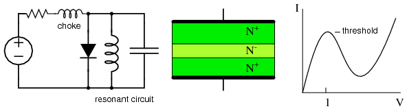
Tunnel diodes
Tunnel diodes exploit a strange quantum phenomenon called resonant tunneling to provide a negative resistance forward-bias characteristics. When a small forward-bias voltage is applied across a tunnel diode, it begins to conduct current. (Figure below(b)) As the voltage is increased, the current increases and reaches a peak value called the peak current (IP). If the voltage is increased a little more, the current actually begins to decrease until it reaches a low point called the valley current (IV). If the voltage is increased further yet, the current begins to increase again, this time without decreasing into another “valley.” The schematic symbol for the tunnel diode shown in Figure below(a).
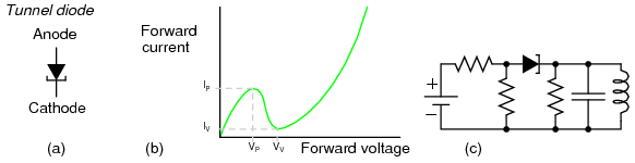
Tunnel diode (a) Schematic symbol. (b) Current vs voltage plot (c) Oscillator.
The forward voltages necessary to drive a tunnel diode to its peak and valley currents are known as peak voltage (VP) and valley voltage (VV), respectively. The region on the graph where current is decreasing while applied voltage is increasing (between VP and VV on the horizontal scale) is known as the region of negative resistance.
Tunnel diodes, also known as Esaki diodes in honor of their Japanese inventor Leo Esaki, are able to transition between peak and valley current levels very quickly, “switching” between high and low states of conduction much faster than even Schottky diodes. Tunnel diode characteristics are also relatively unaffected by changes in temperature.
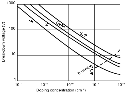
Reverse breakdown voltage versus doping level. After Sze [SGG]
Tunnel diodes are heavily doped in both the P and N regions, 1000 times the level in a rectifier. This can be seen in Figure above. Standard diodes are to the far left, zener diodes near to the left, and tunnel diodes to the right of the dashed line. The heavy doping produces an unusually thin depletion region. This produces an unusually low reverse breakdown voltage with high leakage. The thin depletion region causes high capacitance. To overcome this, the tunnel diode junction area must be tiny. The forward diode characteristic consists of two regions: a normal forward diode characteristic with current rising exponentially beyond VF, 0.3 V for Ge, 0.7 V for Si. Between 0 V and VF is an additional “negative resistance” characteristic peak. This is due to quantum mechanical tunneling involving the dual particle-wave nature of electrons. The depletion region is thin enough compared with the equivalent wavelength of the electron that they can tunnel through. They do not have to overcome the normal forward diode voltage VF. The energy level of the conduction band of the N-type material overlaps the level of the valence band in the P-type region. With increasing voltage, tunneling begins; the levels overlap; current increases, up to a point. As current increases further, the energy levels overlap less; current decreases with increasing voltage. This is the “negative resistance” portion of the curve.
Tunnel diodes are not good rectifiers, as they have relatively high “leakage” current when reverse-biased. Consequently, they find application only in special circuits where their unique tunnel effect has value. To exploit the tunnel effect, these diodes are maintained at a bias voltage somewhere between the peak and valley voltage levels, always in a forward-biased polarity (anode positive, and cathode negative).
Perhaps the most common application of a tunnel diode is in simple high-frequency oscillator circuits as in Figure above(c), where it allows a DC voltage source to contribute power to an LC “tank” circuit, the diode conducting when the voltage across it reaches the peak (tunnel) level and effectively insulating at all other voltages. The resistors bias the tunnel diode at a few tenths of a volt centered on the negative resistance portion of the characteristic curve. The L-C resonant circuit may be a section of a waveguide for microwave operation. Oscillation to 5 GHz is possible.
At one time the tunnel diode was the only solid-state microwave amplifier available. Tunnel diodes were popular starting in the 1960’s. They were longer lived than traveling wave tube amplifiers, an important consideration in satellite transmitters. Tunnel diodes are also resistant to radiation because of the heavy doping. Today various transistors operate at microwave frequencies. Even small signal tunnel diodes are expensive and difficult to find today. There is one remaining manufacturer of germanium tunnel diodes, and none for silicon devices. They are sometimes used in military equipment because they are insensitive to radiation and large temperature changes.
There has been some research involving the possible integration of silicon tunnel diodes into CMOS integrated circuits. They are thought to be capable of switching at 100 GHz in digital circuits. The sole manufacturer of germanium devices produces them one at a time. A batch process for silicon tunnel diodes must be developed, then integrated with conventional CMOS processes. [SZL]
The Esaki tunnel diode should not be confused with the resonant tunneling diode CH 2, of more complex construction from compound semiconductors. The RTD is a more recent development capable of higher speed.
Light-emitting diodes
Diodes, like all semiconductor devices, are governed by the principles described in quantum physics. One of these principles is the emission of specific-frequency radiant energy whenever electrons fall from a higher energy level to a lower energy level. This is the same principle at work in a neon lamp, the characteristic pink-orange glow of ionized neon due to the specific energy transitions of its electrons in the midst of an electric current. The unique color of a neon lamp’s glow is due to the fact that its neon gas inside the tube, and not due to the particular amount of current through the tube or voltage between the two electrodes. Neon gas glows pinkish-orange over a wide range of ionizing voltages and currents. Each chemical element has its own “signature” emission of radiant energy when its electrons “jump” between different, quantized energy levels. Hydrogen gas, for example, glows red when ionized; mercury vapor glows blue. This is what makes spectrographic identification of elements possible.
Electrons flowing through a PN junction experience similar transitions in energy level, and emit radiant energy as they do so. The frequency of this radiant energy is determined by the crystal structure of the semiconductor material, and the elements comprising it. Some semiconductor junctions, composed of special chemical combinations, emit radiant energy within the spectrum of visible light as the electrons change energy levels. Simply put, these junctions glow when forward biased. A diode intentionally designed to glow like a lamp is called a light-emitting diode, or LED.
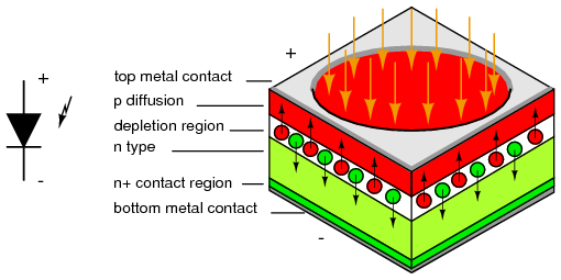
Forward biased silicon diodes give off heat as electron and holes from the N-type and P-type regions, respectively, recombine at the junction. In a forward biased LED, the recombination of electrons and holes in the active region in Figure (c) below (c) yields photons. This process is known as electroluminescence. To give off photons, the potential barrier through which the electrons fall must be higher than for a silicon diode. The forward diode drop can range to a few volts for some color LEDs.
Diodes made from a combination of the elements gallium, arsenic, and phosphorus (called gallium-arsenide-phosphide) glow bright red, and are some of the most common LEDs manufactured. By altering the chemical constituency of the PN junction, different colors may be obtained. Early generations of LEDs were red, green, yellow, orange, and infra-red, later generations included blue and ultraviolet, with violet being the latest color added to the selection. Other colors may be obtained by combining two or more primary-color (red, green, and blue) LEDs together in the same package, sharing the same optical lens. This allowed for multicolor LEDs, such as tricolor LEDs (commercially available in the 1980’s) using red and green (which can create yellow) and later RGB LEDs (red, green, and blue), which cover the entire color spectrum.
The schematic symbol for an LED is a regular diode shape inside of a circle, with two small arrows pointing away (indicating emitted light), shown in Figure (a) below.
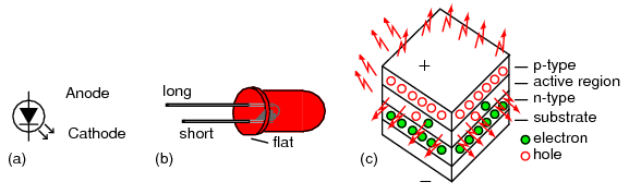
LED, Light Emitting Diode: (a) schematic symbol. (b) Flat side and short lead of device correspond to cathode, as well as the internal arrangement of the cathode. (c) Cross section of Led die.
This notation of having two small arrows pointing away from the device is common to the schematic symbols of all light-emitting semiconductor devices. Conversely, if a device is light-activated (meaning that incoming light stimulates it), then the symbol will have two small arrows pointing toward it. LEDs can sense light. They generate a small voltage when exposed to light, much like a solar cell on a small scale. This property can be gainfully applied in a variety of light-sensing circuits.
Because LEDs are made of different chemical substances than silicon diodes, their forward voltage drops will be different. Typically, LEDs have much larger forward voltage drops than rectifying diodes, anywhere from about 1.6 volts to over 3 volts, depending on the color. Typical operating current for a standard-sized LED is around 20 mA. When operating an LED from a DC voltage source greater than the LED’s forward voltage, a series-connected “dropping” resistor must be included to prevent full source voltage from damaging the LED. Consider the example circuit in Figure (a) below (a) using a 6 V source.
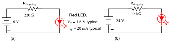
Setting LED current at 20 ma. (a) for a 6 V source, (b) for a 24 V source.
With the LED dropping 1.6 volts, there will be 4.4 volts dropped across the resistor. Sizing the resistor for an LED current of 20 mA is as simple as taking its voltage drop (4.4 volts) and dividing by circuit current (20 mA), in accordance with Ohm’s Law (R=E/I). This gives us a figure of 220 Ω. Calculating power dissipation for this resistor, we take its voltage drop and multiply by its current (P=IE), and end up with 88 mW, well within the rating of a 1/8 watt resistor. Higher battery voltages will require larger-value dropping resistors, and possibly higher-power rating resistors as well. Consider the example in Figure (b) above for a supply voltage of 24 volts:
Here, the dropping resistor must be increased to a size of 1.12 kΩ to drop 22.4 volts at 20 mA so that the LED still receives only 1.6 volts. This also makes for a higher resistor power dissipation: 448 mW, nearly one-half a watt of power! Obviously, a resistor rated for 1/8 watt power dissipation or even 1/4 watt dissipation will overheat if used here.
Dropping resistor values need not be precise for LED circuits. Suppose we were to use a 1 kΩ resistor instead of a 1.12 kΩ resistor in the circuit shown above. The result would be a slightly greater circuit current and LED voltage drop, resulting in a brighter light from the LED and slightly reduced service life. A dropping resistor with too much resistance (say, 1.5 kΩ instead of 1.12 kΩ) will result in less circuit current, less LED voltage, and a dimmer light. LEDs are quite tolerant of variation in applied power, so you need not strive for perfection in sizing the dropping resistor.
Multiple LEDs are sometimes required, say in lighting. If LEDs are operated in parallel, each must have its own current limiting resistor as in Figure (a) below to ensure currents dividing more equally. However, it is more efficient to operate LEDs in series (Figure (b) below with a single dropping resistor. As the number of series LEDs increases the series resistor value must decrease to maintain current, to a point. The number of LEDs in series (Vf) cannot exceed the capability of the power supply. Multiple series strings may be employed as in Figure (c) below.
In spite of equalizing the currents in multiple LEDs, the brightness of the devices may not match due to variations in the individual parts. Parts can be selected for brightness matching for critical applications.
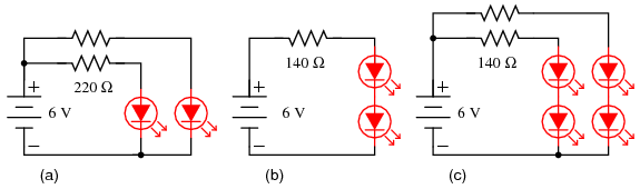
Multiple LEDs: (a) In parallel, (b) in series, (c) series-parallel
Also because of their unique chemical makeup, LEDs have much, much lower peak-inverse voltage (PIV) ratings than ordinary rectifying diodes. A typical LED might only be rated at 5 volts in reverse-bias mode. Therefore, when using alternating current to power an LED, connect a protective rectifying diode anti-parallel with the LED to prevent reverse breakdown every other half-cycle as in Figure (a) below.
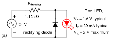
Driving an LED with AC
The anti-parallel diode in Figure (a) above can be replaced with an anti-parallel LED. The resulting pair of anti-parallel LED’s illuminate on alternating half-cycles of the AC sinewave. This configuration draws 20 ma, splitting it equally between the LED’s on alternating AC half cycles. Each LED only receives 10 mA due to this sharing. The same is true of the LED anti-parallel combination with a rectifier. The LED only receives 10 ma. If 20 mA was required for the LED(s), The resistor value could be halved.
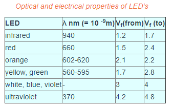
The forward voltage drop of LED’s is inversely proportional to the wavelength (λ). As wavelength decreases going from infrared to visible colors to ultraviolet, Vf increases. While this trend is most obvious in the various devices from a single manufacturer, The voltage range for a particular color LED from various manufacturers varies. This range of voltages is shown in Table below.
As lamps, LEDs are superior to incandescent bulbs in many ways. First and foremost is efficiency: LEDs output far more light power per watt of electrical input than an incandescent lamp. This is a significant advantage if the circuit in question is battery-powered, efficiency translating to longer battery life. Second is the fact that LEDs are far more reliable, having a much greater service life than incandescent lamps. This is because LEDs are “cold” devices: they operate at much cooler temperatures than an incandescent lamp with a white-hot metal filament, susceptible to breakage from mechanical and thermal shock. Third is the high speed at which LEDs may be turned on and off. This advantage is also due to the “cold” operation of LEDs: they don’t have to overcome thermal inertia in transitioning from off to on or vice versa. For this reason, LEDs are used to transmit digital (on/off) information as pulses of light, conducted in empty space or through fiber-optic cable, at very high rates of speed (millions of pulses per second).
LEDs excel in monochromatic lighting applications like traffic signals and automotive tail lights. Incandescents are abysmal in this application since they require filtering, decreasing efficiency. LEDs do not require filtering.
One major disadvantage of using LEDs as sources of illumination is their monochromatic (single-color) emission. No one wants to read a book under the light of a red, green, or blue LED. However, if used in combination, LED colors may be mixed for a more broad-spectrum glow. A new broad spectrum light source is the white LED. While small white panel indicators have been available for many years, illumination grade devices are still in development.
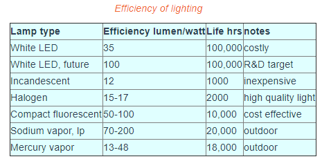
A white LED is a blue LED exciting a phosphor which emits yellow light. The blue plus yellow approximates white light. The nature of the phosphor determines the characteristics of the light. A red phosphor may be added to improve the quality of the yellow plus blue mixture at the expense of efficiency. Table above compares white illumination LEDs to expected future devices and other conventional lamps. Efficiency is measured in lumens of light output per watt of input power. If the 50 lumens/watt device can be improved to 100 lumens/watt, white LEDs will be comparable to compact fluorescent lamps in efficiency.
LEDs in general have been a major subject of R&D since the 1960’s. Because of this it is impractical to cover all geometries, chemistries, and characteristics that have been created over the decades. The early devices were relatively dim and took moderate currents. The efficiencies have been improved in later generations to the point it is hazardous to look closely and directly into an illuminated LED. This can result in eye damage, and the LEDs only required a minor increase in dropping voltage (Vf) and current. Modern high intensity devices have reached 180 lumens using 0.7 Amps (82 lumens/watt, Luxeon Rebel series cool white), and even higher intensity models can use even higher currents with a corresponding increase in brightness. Other developments, such as quantum dots, are the subject of current research, so expect to see new things for these devices in the future.
Laser diodes
The laser diode is a further development upon the regular light-emitting diode, or LED. The term “laser” itself is actually an acronym, despite the fact its often written in lower-case letters. “Laser” stands for Light Amplification by Stimulated Emission of Radiation, and refers to another strange quantum process whereby characteristic light emitted by electrons falling from high-level to low-level energy states in a material stimulate other electrons in a substance to make similar “jumps,” the result being a synchronized output of light from the material. This synchronization extends to the actual phase of the emitted light, so that all light waves emitted from a “lasing” material are not just the same frequency (color), but also the same phase as each other, so that they reinforce one another and are able to travel in a very tightly-confined, nondispersing beam. This is why laser light stays so remarkably focused over long distances: each and every light wave coming from the laser is in step with each other.
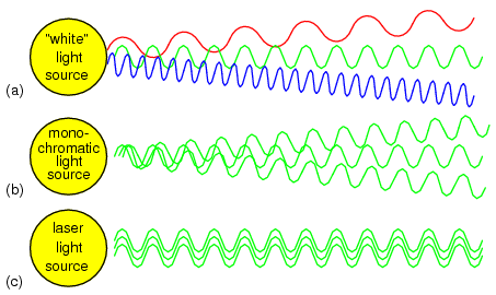
(a) White light of many wavelengths. (b) Mono-chromatic LED light, a single wavelength. (c) Phase coherent laser light.
Incandescent lamps produce “white” (mixed-frequency, or mixed-color) light as in Figure above (a). Regular LEDs produce monochromatic light: same frequency (color), but different phases, resulting in similar beam dispersion in Figure above (b). Laser LEDs produce coherent light: light that is both monochromatic (single-color) and monophasic (single-phase), resulting in precise beam confinement as in Figure above (c).
Laser light finds wide application in the modern world: everything from surveying, where a straight and nondispersing light beam is very useful for precise sighting of measurement markers, to the reading and writing of optical disks, where only the narrowness of a focused laser beam is able to resolve the microscopic “pits” in the disk’s surface comprising the binary 1’s and 0’s of digital information.
Some laser diodes require special high-power “pulsing” circuits to deliver large quantities of voltage and current in short bursts. Other laser diodes may be operated continuously at lower power. In the continuous laser, laser action occurs only within a certain range of diode current, necessitating some form of current-regulator circuit. As laser diodes age, their power requirements may change (more current required for less output power), but it should be remembered that low-power laser diodes, like LEDs, are fairly long-lived devices, with typical service lives in the tens of thousands of hours.
Photodiodes
A photodiode is a diode optimized to produce an electron current flow in response to irradiation by ultraviolet, visible, or infrared light. Silicon is most often used to fabricate photodiodes; though, germanium and gallium arsenide can be used. The junction through which light enters the semiconductor must be thin enough to pass most of the light on to the active region (depletion region) where light is converted to electron hole pairs.
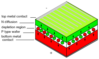
In Figure below a shallow P-type diffusion into an N-type wafer produces a PN junction near the surface of the wafer. The P-type layer needs to be thin to pass as much light as possible. A heavy N+ diffusion on the back of the wafer makes contact with metalization. The top metalization may be a fine grid of metallic fingers on the top of the wafer for large cells. In small photodiodes, the top contact might be a sole bond wire contacting the bare P-type silicon top.
Photodiode: Schematic symbol and cross section.
The intensity of the light entering the top of the photodiode stack falls off exponentially as a function of depth. A thin top P-type layer allows most photons to pass into the depletion region where electron-hole pairs are formed. The electric field across the depletion region due to the built in diode potential causes electrons to be swept into the N-layer, holes into the P-layer. Actually electron-hole pairs may be formed in any of the semiconductor regions. However, those formed in the depletion region are most likely to be separated into the respective N and P-regions. Many of the electron-hole pairs formed in the P and N-regions recombine. Only a few do so in the depletion region. Thus, a few electron-hole pairs in the N and P-regions, and most in the depletion region contribute to photocurrent, that current resulting from light falling on the photodiode.
The voltage out of a photodiode may be observed. Operation in this photovoltaic (PV) mode is not linear over a large dynamic range, though it is sensitive and has low noise at frequencies less than 100 kHz. The preferred mode of operation is often photocurrent (PC) mode because the current is linearly proportional to light flux over several decades of intensity, and higher frequency response can be achieved. PC mode is achieved with reverse bias or zero bias on the photodiode. A current amplifier (transimpedance amplifier) should be used with a photodiode in PC mode. Linearity and PC mode are achieved as long as the diode does not become forward biased.
High speed operation is often required of photodiodes, as opposed to solar cells. Speed is a function of diode capacitance, which can be minimized by decreasing cell area. Thus, a sensor for a high speed fiber optic link will use an area no larger than necessary, say 1 mm2. Capacitance may also be decreased by increasing the thickness of the depletion region, in the manufacturing process or by increasing the reverse bias on the diode.
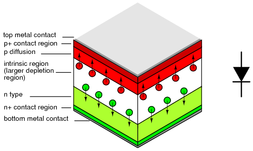
PIN diode The p-i-n diode or PIN diode is a photodiode with an intrinsic layer between the P and N-regions as in Figure below. The P-Intrinsic-N structure increases the distance between the P and N conductive layers, decreasing capacitance, increasing speed. The volume of the photo sensitive region also increases, enhancing conversion efficiency. The bandwidth can extend to 10’s of gHz. PIN photodiodes are the preferred for high sensitivity, and high speed at moderate cost.
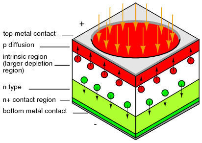
PIN photodiode: The intrinsic region increases the thickness of the depletion region.
Avalanche photo diode:An avalanche photodiode (APD)designed to operate at high reverse bias exhibits an electron multiplier effect analogous to a photomultiplier tube. The reverse bias can run from 10’s of volts to nearly 2000 V. The high level of reverse bias accelerates photon created electron-hole pairs in the intrinsic region to a high enough velocity to free additional carriers from collisions with the crystal lattice. Thus, many electrons per photon result. The motivation for the APD is to achieve amplification within the photodiode to overcome noise in external amplifiers. This works to some extent. However, the APD creates noise of its own. At high speed the APD is superior to a PIN diode amplifier combination, though not for low speed applications. APD’s are expensive, roughly the price of a photomultiplier tube. So, they are only competitive with PIN photodiodes for niche applications. One such application is single photon counting as applied to nuclear physics.
Solar cells
A photodiode optimized for efficiently delivering power to a load is the solar cell. It operates in photovoltaic mode (PV) because it is forward biased by the voltage developed across the load resistance.
Monocrystalline solar cells are manufactured in a process similar to semiconductor processing. This involves growing a single crystal boule from molten high purity silicon (P-type), though, not as high purity as for semiconductors. The boule is diamond sawed or wire sawed into wafers. The ends of the boule must be discarded or recycled, and silicon is lost in the saw kerf. Since modern cells are nearly square, silicon is lost in squaring the boule. Cells may be etched to texture (roughen) the surface to help trap light within the cell. Considerable silicon is lost in producing the 10 or 15 cm square wafers. These days (2007) it is common for solar cell manufacturer to purchase the wafers at this stage from a supplier to the semiconductor industry.
P-type Wafers are loaded back-to-back into fused silica boats exposing only the outer surface to the N-type dopant in the diffusion furnace. The diffusion process forms a thin n-type layer on the top of the cell. The diffusion also shorts the edges of the cell front to back. The periphery must be removed by plasma etching to unshort the cell. Silver and or aluminum paste is screened on the back of the cell, and a silver grid on the front. These are sintered in a furnace for good electrical contact. (Figure below)
The cells are wired in series with metal ribbons. For charging 12 V batteries, 36 cells at approximately 0.5 V are vacuum laminated between glass, and a polymer metal back. The glass may have a textured surface to help trap light.
Silicon Solar cell
The ultimate commercial high efficiency (21.5%) single crystal silicon solar cells have all contacts on the back of the cell. The active area of the cell is increased by moving the top (-) contact conductors to the back of the cell. The top (-) contacts are normally made to the N-type silicon on top of the cell. In Figure below the (-) contacts are made to N+ diffusions on the bottom interleaved with (+) contacts. The top surface is textured to aid in trapping light within the cell.
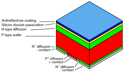
High efficiency solar cell with all contacts on the back. Adapted from Figure 1
Multicyrstalline silicon cells start out as molten silicon cast into a rectangular mold. As the silicon cools, it crystallizes into a few large (mm to cm sized) randomly oriented crystals instead of a single one. The remainder of the process is the same as for single crystal cells. The finished cells show lines dividing the individual crystals, as if the cells were cracked. The high efficiency is not quite as high as single crystal cells due to losses at crystal grain boundaries. The cell surface cannot be roughened by etching due to the random orientation of the crystals. However, an antireflectrive coating improves efficiency. These cells are competitive for all but space applications.
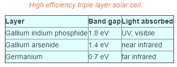
Three layer cell: The highest efficiency solar cell is a stack of three cells tuned to absorb different portions of the solar spectrum. Though three cells can be stacked atop one another, a monolithic single crystal structure of 20 semiconductor layers is more compact. At 32 % efficiency, it is now (2007) favored over silicon for space application. The high cost prevents it from finding many earth bound applications other than concentrators based on lenses or mirrors.
Intensive research has recently produced a version enhanced for terrestrial concentrators at 400 - 1000 suns and 40.7% efficiency. This requires either a big inexpensive Fresnel lens or reflector and a small area of the expensive semiconductor. This combination is thought to be competitive with inexpensive silicon cells for solar power plants. [RRK] [LZy]
Metal organic chemical vapor deposition (MOCVD) deposits the layers atop a P-type germanium substrate. The top layers of N and P-type gallium indium phosphide (GaInP) having a band gap of 1.85 eV, absorbs ultraviolet and visible light. These wavelengths have enough energy to exceed the band gap. Longer wavelengths (lower energy) do not have enough energy to create electron-hole pairs, and pass on through to the next layer. A gallium arsenide layers having a band gap of 1.42 eV, absorbs near infrared light. Finally the germanium layer and substrate absorb far infrared. The series of three cells produce a voltage which is the sum of the voltages of the three cells. The voltage developed by each material is 0.4 V less than the band gap energy listed in Table below. For example, for GaInP: 1.8 eV/e - 0.4 V = 1.4 V. For all three the voltage is 1.4 V + 1.0 V + 0.3 V = 2.7 V.
Crystalline solar cell arrays have a long usable life. Many arrays are guaranteed for 25 years, and believed to be good for 40 years. They do not suffer initial degradation compared with amorphous silicon.
Both single and multicrystalline solar cells are based on silicon wafers. The silicon is both the substrate and the active device layers. Much silicon is consumed. This kind of cell has been around for decades, and takes approximately 86% of the solar electric market. For further information about crystalline solar cells see Honsberg. [CHS]
Amorphous silicon thin film solar cells use tiny amounts of the active raw material, silicon. Approximately half the cost of conventional crystalline solar cells is the solar cell grade silicon. The thin film deposition process reduces this cost. The downside is that efficiency is about half that of conventional crystalline cells. Moreover, efficiency degrades by 15-35% upon exposure to sunlight. A 7% efficient cell soon ages to 5% efficiency. Thin film amorphous silicon cells work better than crystalline cells in dim light. They are put to good use in solar powered calculators.
Non-silicon based solar cells make up about 7% of the market. These are thin-film polycrystalline products. Various compound semiconductors are the subject of research and development. Some non-silicon products are in production. Generally, the efficiency is better than amorphous silicon, but not nearly as good as crystalline silicon.
Cadmium telluride as a polycrystalline thin film on metal or glass can have a higher efficiency than amorphous silicon thin films. If deposited on metal, that layer is the negative contact to the cadmium telluride thin film. The transparent P-type cadmium sulfide atop the cadmium telluride serves as a buffer layer. The positive top contact is transparent, electrically conductive fluorine doped tin oxide. These layers may be laid down on a sacrificial foil in place of the glass in the process in the following pargraph. The sacrificial foil is removed after the cell is mounted to a permanent substrate.
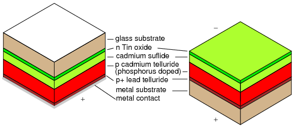
Cadmium telluride solar cell on glass or metal.
A process for depositing cadmium telluride on glass begins with the deposition of N-type transparent, electrically conducive, tin oxide on a glass substrate. The next layer is P-type cadmium telluride; though, N-type or intrinsic may be used. These two layers constitute the NP junction. A P+ (heavy P-type) layer of lead telluride aids in establishing a low resistance contact. A metal layer makes the final contact to the lead telluride. These layers may be laid down by vacuum deposition, chemical vapor deposition (CVD), screen printing, electrodeposition, or atmospheric pressure chemical vapor deposition (APCVD) in helium. [KWM]
A variation of cadmium telluride is mercury cadmium telluride. Having lower bulk resistance and lower contact resistance improves efficiency over cadmium telluride.
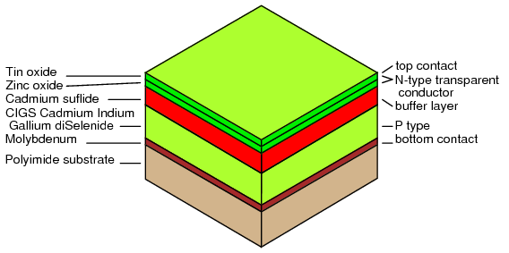
Cadmium Indium Gallium diSelenide solar cell (CIGS)
Cadmium Indium Gallium diSelenide: A most promising thin film solar cell at this time (2007) is manufactured on a ten inch wide roll of flexible polyimide– Cadmium Indium Gallium diSelenide (CIGS). It has a spectacular efficiency of 10%. Though, commercial grade crystalline silicon cells surpassed this decades ago, CIGS should be cost competitive. The deposition processes are at a low enough temperature to use a polyimide polymer as a substrate instead of metal or glass. (Figure above) The CIGS is manufactured in a roll to roll process, which should drive down costs. GIGS cells may also be produced by an inherently low cost electrochemical process. [EET]
REVIEW:
- Most solar cells are silicon single crystal or multicrystal because of their good efficiency and moderate cost.
- Less efficient thin films of various amorphous or polycrystalline materials comprise the rest of the market.
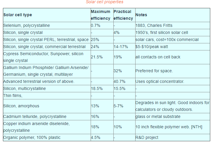
- Table below compares selected solar cells.
Varicap or varactor diodes
A variable capacitance diode is known as a varicap diode or as a varactor. If a diode is reverse biased, an insulating depletion region forms between the two semiconductive layers. In many diodes the width of the depletion region may be changed by varying the reverse bias. This varies the capacitance. This effect is accentuated in varicap diodes. The schematic symbols is shown in Figure below, one of which is packaged as common cathode dual diode.
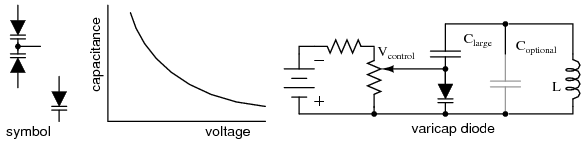
Varicap diode: Capacitance varies with reverse bias. This varies the frequency of a resonant network.
If a varicap diode is part of a resonant circuit as in Figure above, the frequency may be varied with a control voltage, Vcontrol. A large capacitance, low Xc, in series with the varicap prevents Vcontrol from being shorted out by inductor L. As long as the series capacitor is large, it has minimal effect on the frequency of resonant circuit. Coptional may be used to set the center resonant frequency. Vcontrol can then vary the frequency about this point. Note that the required active circuitry to make the resonant network oscillate is not shown. For an example of a varicap diode tuned AM radio receiver see “electronic varicap diode tuning,” Ch 9
Some varicap diodes may be referred to as abrupt, hyperabrupt, or super hyper abrupt. These refer to the change in junction capacitance with changing reverse bias as being abrupt or hyper-abrupt, or super hyperabrupt. These diodes offer a relatively large change in capacitance. This is useful when oscillators or filters are swept over a large frequency range. Varying the bias of abrupt varicaps over the rated limits, changes capacitance by a 4:1 ratio, hyperabrupt by 10:1, super hyperabrupt by 20:1.
Varactor diodes may be used in frequency multiplier circuits. See “Practical analog semiconductor circuits,” Varactor multiplier
Snap diode
The snap diode, also known as the step recovery diode is designed for use in high ratio frequency multipliers up to 20 gHz. When the diode is forward biased, charge is stored in the PN junction. This charge is drawn out as the diode is reverse biased. The diode looks like a low impedance current source during forward bias. When reverse bias is applied it still looks like a low impedance source until all the charge is withdrawn. It then “snaps” to a high impedance state causing a voltage impulse, rich in harmonics. An applications is a comb generator, a generator of many harmonics. Moderate power 2x and 4x multipliers are another application.
PIN diodes
A PIN diode is a fast low capacitance switching diode. Do not confuse a PIN switching diode with a PIN photo diode. A PIN diode is manufactured like a silicon switching diode with an intrinsic region added between the PN junction layers. This yields a thicker depletion region, the insulating layer at the junction of a reverse biased diode. This results in lower capacitance than a reverse biased switching diode.
Pin diode: Cross section aligned with schematic symbol.
PIN diodes are used in place of switching diodes in radio frequency (RF) applications, for example, a T/R switch. The 1n4007 1000 V, 1 A general purpose power diode is reported to be usable as a PIN switching diode. The high voltage rating of this diode is achieved by the inclusion of an intrinsic layer dividing the PN junction. This intrinsic layer makes the 1n4007 a PIN diode. Another PIN diode application is as the antenna switch here for a direction finder receiver.
PIN diodes serve as variable resistors when the forward bias is varied. One such application is the voltage variable attenuator. The low capacitance characteristic of PIN diodes, extends the frequency flat response of the attenuator to microwave frequencies.
IMPATT diode
IMPact Avalanche Transit Time diode is a high power radio frequency (RF) generator operating from 3 to 100 gHz. IMPATT diodes are fabricated from silicon, gallium arsenide, or silicon carbide.
An IMPATT diode is reverse biased above the breakdown voltage. The high doping levels produce a thin depletion region. The resulting high electric field rapidly accelerates carriers which free other carriers in collisions with the crystal lattice. Holes are swept into the P+ region. Electrons drift toward the N regions. The cascading effect creates an avalanche current which increases even as voltage across the junction decreases. The pulses of current lag the voltage peak across the junction. A “negative resistance” effect in conjunction with a resonant circuit produces oscillations at high power levels (high for semiconductors).
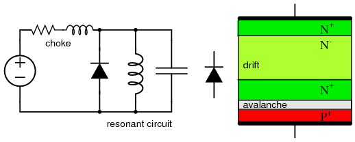
IMPATT diode: Oscillator circuit and heavily doped P and N layers.
The resonant circuit in the schematic diagram of Figure above is the lumped circuit equivalent of a waveguide section, where the IMPATT diode is mounted. DC reverse bias is applied through a choke which keeps RF from being lost in the bias supply. This may be a section of waveguide known as a bias Tee. Low power RADAR transmitters may use an IMPATT diode as a power source. They are too noisy for use in the receiver. [ YMCW]
Gunn diode
Diode, gunn Gunn diode
A gunn diode is solely composed of N-type semiconductor. As such, it is not a true diode. Figure below shows a lightly doped N- layer surrounded by heavily doped N+ layers. A voltage applied across the N-type gallium arsenide gunn diode creates a strong electric field across the lightly doped N- layer.
Gunn diode: Oscillator circuit and cross section of only N-type semiconductor diode.
As voltage is increased, conduction increases due to electrons in a low energy conduction band. As voltage is increased beyond the threshold of approximately 1 V, electrons move from the lower conduction band to the higher energy conduction band where they no longer contribute to conduction. In other words, as voltage increases, current decreases, a negative resistance condition. The oscillation frequency is determined by the transit time of the conduction electrons, which is inversely related to the thickness of the N- layer.
The frequency may be controlled to some extent by embedding the gunn diode into a resonant circuit. The lumped circuit equivalent shown in Figure above is actually a coaxial transmission line or waveguide. Gallium arsenide gunn diodes are available for operation from 10 to 200 gHz at 5 to 65 mw power. Gunn diodes may also serve as amplifiers. [CHW] [IAP]
Shockley diode
The Shockley diode is a 4-layer thyristor used to trigger larger thyristors. It only conducts in one direction when triggered by a voltage exceeding the breakover voltage, about 20 V. See “Thyristors,” The Shockley Diode. The bidirectional version is called a diac. See “Thyristors,” The DIAC.
Constant-current diodes
A constant-current diode, also known as a current-limiting diode, or current-regulating diode, does exactly what its name implies: it regulates current through it to some maximum level. The constant current diode is a two terminal version of a JFET. If we try to force more current through a constant-current diode than its current-regulation point, it simply “fights back” by dropping more voltage. If we were to build the circuit in Figure below(a) and plot diode current against diode voltage, we’d get a graph that rises at first and then levels off at the current regulation point as in Figure below(b).
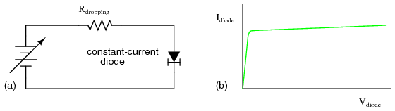
Constant current diode: (a) Test circuit, (b) current vs voltage characteristic.
One application for a constant-current diode is to automatically limit current through an LED or laser diode over a wide range of power supply voltages as in Figure below.
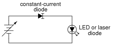
Constant current diode application: driving laser diode.
Of course, the constant-current diode’s regulation point should be chosen to match the LED or laser diode’s optimum forward current. This is especially important for the laser diode, not so much for the LED, as regular LEDs tend to be more tolerant of forward current variations.