
7.5: NAND Gate S-R Flip-Flop
- Page ID
- 1282

\( \newcommand{\vecs}[1]{\overset { \scriptstyle \rightharpoonup} {\mathbf{#1}} } \)
\( \newcommand{\vecd}[1]{\overset{-\!-\!\rightharpoonup}{\vphantom{a}\smash {#1}}} \)
\( \newcommand{\dsum}{\displaystyle\sum\limits} \)
\( \newcommand{\dint}{\displaystyle\int\limits} \)
\( \newcommand{\dlim}{\displaystyle\lim\limits} \)
\( \newcommand{\id}{\mathrm{id}}\) \( \newcommand{\Span}{\mathrm{span}}\)
( \newcommand{\kernel}{\mathrm{null}\,}\) \( \newcommand{\range}{\mathrm{range}\,}\)
\( \newcommand{\RealPart}{\mathrm{Re}}\) \( \newcommand{\ImaginaryPart}{\mathrm{Im}}\)
\( \newcommand{\Argument}{\mathrm{Arg}}\) \( \newcommand{\norm}[1]{\| #1 \|}\)
\( \newcommand{\inner}[2]{\langle #1, #2 \rangle}\)
\( \newcommand{\Span}{\mathrm{span}}\)
\( \newcommand{\id}{\mathrm{id}}\)
\( \newcommand{\Span}{\mathrm{span}}\)
\( \newcommand{\kernel}{\mathrm{null}\,}\)
\( \newcommand{\range}{\mathrm{range}\,}\)
\( \newcommand{\RealPart}{\mathrm{Re}}\)
\( \newcommand{\ImaginaryPart}{\mathrm{Im}}\)
\( \newcommand{\Argument}{\mathrm{Arg}}\)
\( \newcommand{\norm}[1]{\| #1 \|}\)
\( \newcommand{\inner}[2]{\langle #1, #2 \rangle}\)
\( \newcommand{\Span}{\mathrm{span}}\) \( \newcommand{\AA}{\unicode[.8,0]{x212B}}\)
\( \newcommand{\vectorA}[1]{\vec{#1}} % arrow\)
\( \newcommand{\vectorAt}[1]{\vec{\text{#1}}} % arrow\)
\( \newcommand{\vectorB}[1]{\overset { \scriptstyle \rightharpoonup} {\mathbf{#1}} } \)
\( \newcommand{\vectorC}[1]{\textbf{#1}} \)
\( \newcommand{\vectorD}[1]{\overrightarrow{#1}} \)
\( \newcommand{\vectorDt}[1]{\overrightarrow{\text{#1}}} \)
\( \newcommand{\vectE}[1]{\overset{-\!-\!\rightharpoonup}{\vphantom{a}\smash{\mathbf {#1}}}} \)
\( \newcommand{\vecs}[1]{\overset { \scriptstyle \rightharpoonup} {\mathbf{#1}} } \)
\(\newcommand{\longvect}{\overrightarrow}\)
\( \newcommand{\vecd}[1]{\overset{-\!-\!\rightharpoonup}{\vphantom{a}\smash {#1}}} \)
\(\newcommand{\avec}{\mathbf a}\) \(\newcommand{\bvec}{\mathbf b}\) \(\newcommand{\cvec}{\mathbf c}\) \(\newcommand{\dvec}{\mathbf d}\) \(\newcommand{\dtil}{\widetilde{\mathbf d}}\) \(\newcommand{\evec}{\mathbf e}\) \(\newcommand{\fvec}{\mathbf f}\) \(\newcommand{\nvec}{\mathbf n}\) \(\newcommand{\pvec}{\mathbf p}\) \(\newcommand{\qvec}{\mathbf q}\) \(\newcommand{\svec}{\mathbf s}\) \(\newcommand{\tvec}{\mathbf t}\) \(\newcommand{\uvec}{\mathbf u}\) \(\newcommand{\vvec}{\mathbf v}\) \(\newcommand{\wvec}{\mathbf w}\) \(\newcommand{\xvec}{\mathbf x}\) \(\newcommand{\yvec}{\mathbf y}\) \(\newcommand{\zvec}{\mathbf z}\) \(\newcommand{\rvec}{\mathbf r}\) \(\newcommand{\mvec}{\mathbf m}\) \(\newcommand{\zerovec}{\mathbf 0}\) \(\newcommand{\onevec}{\mathbf 1}\) \(\newcommand{\real}{\mathbb R}\) \(\newcommand{\twovec}[2]{\left[\begin{array}{r}#1 \\ #2 \end{array}\right]}\) \(\newcommand{\ctwovec}[2]{\left[\begin{array}{c}#1 \\ #2 \end{array}\right]}\) \(\newcommand{\threevec}[3]{\left[\begin{array}{r}#1 \\ #2 \\ #3 \end{array}\right]}\) \(\newcommand{\cthreevec}[3]{\left[\begin{array}{c}#1 \\ #2 \\ #3 \end{array}\right]}\) \(\newcommand{\fourvec}[4]{\left[\begin{array}{r}#1 \\ #2 \\ #3 \\ #4 \end{array}\right]}\) \(\newcommand{\cfourvec}[4]{\left[\begin{array}{c}#1 \\ #2 \\ #3 \\ #4 \end{array}\right]}\) \(\newcommand{\fivevec}[5]{\left[\begin{array}{r}#1 \\ #2 \\ #3 \\ #4 \\ #5 \\ \end{array}\right]}\) \(\newcommand{\cfivevec}[5]{\left[\begin{array}{c}#1 \\ #2 \\ #3 \\ #4 \\ #5 \\ \end{array}\right]}\) \(\newcommand{\mattwo}[4]{\left[\begin{array}{rr}#1 \amp #2 \\ #3 \amp #4 \\ \end{array}\right]}\) \(\newcommand{\laspan}[1]{\text{Span}\{#1\}}\) \(\newcommand{\bcal}{\cal B}\) \(\newcommand{\ccal}{\cal C}\) \(\newcommand{\scal}{\cal S}\) \(\newcommand{\wcal}{\cal W}\) \(\newcommand{\ecal}{\cal E}\) \(\newcommand{\coords}[2]{\left\{#1\right\}_{#2}}\) \(\newcommand{\gray}[1]{\color{gray}{#1}}\) \(\newcommand{\lgray}[1]{\color{lightgray}{#1}}\) \(\newcommand{\rank}{\operatorname{rank}}\) \(\newcommand{\row}{\text{Row}}\) \(\newcommand{\col}{\text{Col}}\) \(\renewcommand{\row}{\text{Row}}\) \(\newcommand{\nul}{\text{Nul}}\) \(\newcommand{\var}{\text{Var}}\) \(\newcommand{\corr}{\text{corr}}\) \(\newcommand{\len}[1]{\left|#1\right|}\) \(\newcommand{\bbar}{\overline{\bvec}}\) \(\newcommand{\bhat}{\widehat{\bvec}}\) \(\newcommand{\bperp}{\bvec^\perp}\) \(\newcommand{\xhat}{\widehat{\xvec}}\) \(\newcommand{\vhat}{\widehat{\vvec}}\) \(\newcommand{\uhat}{\widehat{\uvec}}\) \(\newcommand{\what}{\widehat{\wvec}}\) \(\newcommand{\Sighat}{\widehat{\Sigma}}\) \(\newcommand{\lt}{<}\) \(\newcommand{\gt}{>}\) \(\newcommand{\amp}{&}\) \(\definecolor{fillinmathshade}{gray}{0.9}\)PARTS AND MATERIALS
- 4011 quad NAND gate (Radio Shack catalog # 276-2411)
- 4001 quad NOR gate (Radio Shack catalog # 276-2401)
- Eight-position DIP switch (Radio Shack catalog # 275-1301)
- Ten-segment bar graph LED (Radio Shack catalog # 276-081)
- One 6 volt battery
- Three 10 kΩ resistors
- Two 470 Ω resistors
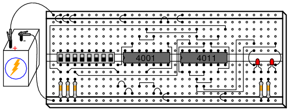
Caution! The 4011 IC is CMOS, and therefore sensitive to static electricity! Although the parts list calls for a ten-segment LED unit, the illustration shows two individual LEDs being used instead. This is due to lack of room on my breadboard to mount the switch assembly, two integrated circuits, and the bar graph. If you have room on your breadboard, feel free to use the bar graph as called for in the parts list, and as shown in prior latch circuits.
CROSS-REFERENCES
Lessons In Electric Circuits, Volume 4, chapter 3: “Logic Gates”
Lessons In Electric Circuits, Volume 4, chapter 10: “Multivibrators”
LEARNING OBJECTIVES
- The difference between a gated latch and a flip-flop
- How to build a “pulse detector” circuit
- Learn the effects of switch contact “bounce” on digital circuits
SCHEMATIC DIAGRAM
ILLUSTRATION
INSTRUCTIONS
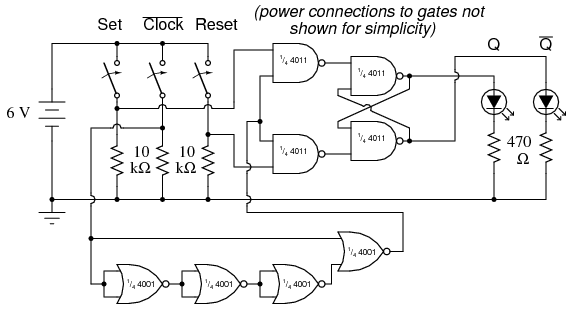
The only difference between a gated (or enabled) latch and a flip-flop is that a flip-flop is enabled only on the rising or falling edge of a “clock” signal, rather than for the entire duration of a “high” enable signal. Converting an enabled latch into a flip-flop simply requires that a “pulse detector” circuit be added to the Enable input so that the edge of a clock pulse generates a brief “high” Enable pulse:
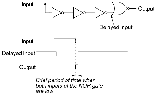
The single NOR gate and three inverter gates create this effect by exploiting the propagation delay time of multiple, cascaded gates. In this experiment, I use three NOR gates with paralleled inputs to create three inverters, thus using all four NOR gates of a 4001 integrated circuit:
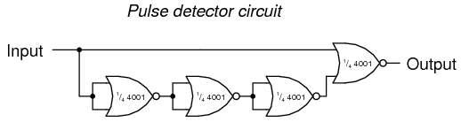
Normally, when using a NOR gate as an inverter, one input would be grounded while the other acts as the inverter input, to minimize input capacitance and increase speed. Here, however, slow response is desired, and so I parallel the NOR inputs to make inverters rather than use the more conventional method. Please note that this particular pulse detector circuit produces a “high” output pulse at every falling edge of the clock (input) signal. This means that the flip-flop circuit should be responsive to the Set and Reset input states only when the middle switch is moved from “on” to “off,” not from “off” to “on.”
When you build this circuit, though, you may discover that the outputs respond to Set and Reset input signals during both transitions of the Clock input, not just when it is switched from a “high” state to a “low” state. The reason for this is contact bounce: the effect of a mechanical switch rapidly making-and-breaking when its contacts are first closed, due to the elastic collision of the metal contact pads. Instead of the Clock switch producing a single, clean low-to-high signal transition when closed, there will most likely be several low-high-low “cycles” as the contact pads “bounce” upon off-to-on actuation. The first high-to-low transition caused by bouncing will trigger the pulse detector circuit, enabling the S-R latch for that moment in time, making it responsive to the Set and Reset inputs. Ideally, of course, switches are perfect and bounce-free. In the real world, though, contact bounce is a very common problem for digital gate circuits operated by switch inputs and must be understood well if it is to be overcome.